
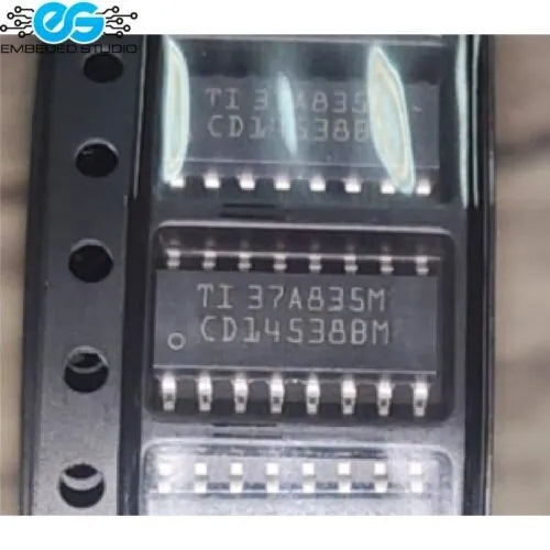
CD14538BM dual monostable multivibrator IC — retriggerable, CMOS B-series, SOP-16
The CD14538BM is a dual precision monostable multivibrator (one-shot) IC from the CMOS B-series, housed in the SOP-16 SMD package. Each of the two independent monostable circuits is retriggerable and resettable, with separate trigger and reset inputs, making it highly flexible for pulse timing, pulse delay, and pulse shaping applications in digital and mixed-signal systems.
The Schmitt-trigger inputs on the +TR and −TR pins allow triggering from signals with unlimited rise and fall times, eliminating the need for signal conditioning on slow or noisy input edges. The device operates from a wide supply range of 3V to 18V, with 5V, 10V, and 15V parametric ratings, and meets all JEDEC B-series CMOS specifications. It is a direct replacement for the CD4538B.
Key Specifications:
- Part number: CD14538BM
- Channels: 2 (dual, independent monostable multivibrators)
- Supply voltage (VDD): 3V – 18V
- Parametric ratings: 5V, 10V, 15V
- Trigger inputs: Schmitt-trigger (+TR and −TR), leading or trailing edge selectable
- Retriggerable: yes
- Resettable: yes (separate reset per channel)
- Outputs: Q and Q̅ (buffered, both available)
- Maximum input current: 1μA at 18V (full temperature range)
- Noise margin: 1V @ 5V, 2V @ 10V, 2.5V @ 15V
- Package: SOP-16 (SMD, 16-pin)
- Replaces: CD4538B
Key Features:
- Dual independent monostable circuits — two one-shot timers in a single package
- Retriggerable — output pulse can be extended by re-triggering before timeout
- Schmitt-trigger inputs — tolerates slow, noisy, or undefined-slope input signals without false triggering
- Leading or trailing edge trigger — selectable via +TR or −TR input for maximum flexibility
- Separate resets per channel — independent reset control for each monostable
- Q and Q̅ outputs — both true and complementary outputs available
- Wide supply range (3V–18V) — compatible with 3.3V, 5V, and 12V systems
- Direct CD4538B replacement — drop-in compatible
Applications:
- Pulse delay and timing circuits
- Pulse width generation and shaping
- Debounce circuits for mechanical switches
- Missing pulse detector
- Frequency divider and clock gating
- Edge-to-pulse conversion
- Watchdog timer circuits
Note: Pulse width is set by an external resistor (RX) and capacitor (CX): tW ≈ RX × CX. Trigger and reset propagation delays are independent of RX and CX values. Refer to the CD14538BM datasheet for timing diagrams and RX/CX selection guidelines.


