IC and IC Sockets
Showing 16–30 of 95 results
-
IC and IC Sockets
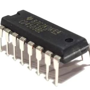
CD14538BE DIP
- An unused RESET input should be tied to VDD
- Trigger and reset propagation delays independent of RX, CX
- Triggering from leading or trailing edge
- Separate resets, replaces CD4538B Type
- Wide range of output-pulse widths
- Schmitt-trigger input allows unlimited rise and fall times on +TR and -TR inputs
- 100% tested for maximum quiescent current at 20 V
- Standardized, symmetrical output characteristics
- Supply voltage range from 3 to 18V (at full operating temperature)
- 16 pin PDIP package, operating temperature range from -55 to 125°C
SKU: n/a -
IC and IC Sockets
CD14538BM SOP
CD14538BM SOP Features:
- Retriggerable/resettable capability
- Trigger and reset propagation delays independent of RX, CX
- Triggering from leading or trailing edge
- Q and Q\ buffered outputs available
- Separate resets
- Replaces CD4538B Type
- Wide range of output-pulse widths
- Schmitt-trigger input allows unlimited rise and fall times on +TR and -TR inputs
- 100% tested for maximum quiescent current at 20 V
- Maximum input current of 1 µA at 18 V over full package-temperature range; 100 nA at 18 V and 25°C
SKU: n/a -
IC and IC Sockets
CD40106BE IC
Features:
1• Schmitt-Trigger Inputs
• Hysteresis Voltage (Typical):
– 0.9 V at VDD = 5 V
– 2.3 V at VDD = 10 V
– 3.5 V at VDD = 15 V
• Noise Immunity Greater Than 50%
• No Limit On Input Rise and Fall Times
• Standardized, Symmetrical Output Characteristics
• For Quiescent Current at 20 V
• Maximum Input Current Of 1 μA at 18 V Over Full
Package Temperature Range:
– 100 nA at 18 V and 25°C
• Low VDD and VSS Current During Slow Input
Ramp
• 5-V, 10-V, and 15-V Parametric RatingsSKU: n/a -
IC and IC Sockets
CD40106BM SOP
Features
1• Schmitt-Trigger Inputs
• Hysteresis Voltage (Typical):
– 0.9 V at VDD = 5 V
– 2.3 V at VDD = 10 V
– 3.5 V at VDD = 15 V
• Noise Immunity Greater Than 50%
• No Limit On Input Rise and Fall Times
• Standardized, Symmetrical Output Characteristics
• For Quiescent Current at 20 V
• Maximum Input Current Of 1 μA at 18 V Over Full
Package Temperature Range:
– 100 nA at 18 V and 25°C
• Low VDD and VSS Current During Slow Input
Ramp
• 5-V, 10-V, and 15-V Parametric RatingsSKU: n/a -
IC and IC Sockets
CD4049BE DIP
Features:
- Dip-16 Package
- High Sink Current for Driving 2 TTL Loads
- High-To-Low Level Logic Conversion
- Maximum Input Current of 1uA at 18V Over Full Package Temperature Range
- 5V, 10V and 15V Parametric Ratings
- CD4049UB Inverting
• CD4050B Noninverting
• High Sink Current for Driving 2 TTL Loads
• High-to-Low Level Logic Conversion
• 100% Tested for Quiescent Current at 20 V
• Maximum Input Current of 1 µA at 18 V Over Full Package Temperature Range; 100 nA at 18 V and 25°C
• 5-V, 10-V, and 15-V Parametric Ratings
SKU: n/a -
IC and IC Sockets
CD4049BM SOP
Features:- CD4049UB Inverting
- CD4050B Noninverting
- High Sink Current for Driving 2 TTL Loads
- High-to-Low Level Logic Conversion
- 100% Tested for Quiescent Current at 20 V
- Maximum Input Current of 1 µA at 18 V Over Full Package
- Temperature Range; 100 nA at 18 V and 25°C
- 5-V, 10-V, and 15-V Parametric Ratings
SKU: n/a -
IC and IC Sockets
CD4093BE IC CMOS
The product consists of four Schmitt-trigger circuits. Each circuit functions as a two-input NAND gate with Schmitt-trigger action on both inputs. The gate switches at different points for positive- and negative-going signals. The difference between the positive voltage (VP) and the negative voltage (VN) is defined as hysteresis voltage (VH)
SKU: n/a -
IC and IC Sockets
CD4503BE IC CMOS
Technical Specifications:
- Logic Family: CMOS
- Number of Buffers: 6
- Supply Voltage Range: 3V to 15V
- High-Level Output Current (I_OH): -4 mA
- Low-Level Output Current (I_OL): 4 mA
- High-Level Input Voltage (V_IH): 0.7 V_DD min
- Low-Level Input Voltage (V_IL): 0.3 V_DD max
- Propagation Delay Time: 250 ns (typical) at V_DD = 10V
- Power Dissipation: 500 mW (max)
SKU: n/a -
IC and IC Sockets
CD4503BM SOP
The CD4503BM is a Hex Non-inverting Buffer with 3-state outputs having high sink and source-current capability. Two disable controls are provided, one of which controls four buffers and the other controls the remaining two buffers.
- 1 TTL-load output drive capability
- 2 Output-disable controls
- Pin compatible with industry types MM80C97, MC14503 and 340097
- 5/10/15V Parametric ratings
- Meets all requirements of JEDEC tentative standard no. 13B
- Green product and no Sib/Br
Applications
Industrial, Automation & Process Control, Signal Processing
SKU: n/a -
IC and IC Sockets
D151821-0571 IC
The D151821-0571 is an integrated circuit (IC) from NEC. It is a low-power, low-voltage, high-speed CMOS logic device with a 24-pin small outline package (SOP). Features: Low power consumption Low voltage operation High speed operation 24-pin SOP package High noise immunity Low input and output leakage current High noise margin Applications: The D151821-0571 is suitable for a wide range of applications including logic gates, logic buffers, and other logic functions. It can be used in consumer electronics, automotive, industrial, and medical applications.
SKU: n/a -
IC and IC Sockets
EUP3482 SOP
FEATURES
2A Output Current
220ns Minimum On Time
35V Input Surge Protection
Integrated 160mΩ/110mΩ DMOS Switches
4.5V to 30V Input Operating Range
Output Adjustable from 0.923V to 20V
Up to 95% Efficiency
1µA Shutdown Current
Fixed 340KHz Frequency
Programmable Soft-Start
Thermal Shutdown and Overcurrent Protection
Input Supply Overvoltage and Undervoltage
Lockout
Available in SOP-8 PackageSKU: n/a -
IC and IC Sockets
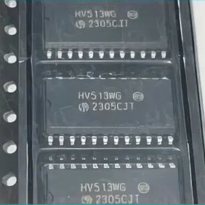
HV513WG SOP-24
HV513WG SOP-24 Features
- Up to 250V Output Voltage
- Low-Power Level Shifting from 5V to 250V
- Shift Register Speed:
– 8 MHz at VDD = 5V - Latched Data Outputs
- Output Polarity and Blanking
- Output Short-Circuit Detect
- Output High-Z (Hi-Z) Control
- CMOS-Compatible Inputs
SKU: n/a -
-
IC and IC Sockets
L6384D SOP
L6384D Features:
- (1)high voltage rail up to 600 V;
- (2)dV/dt immunity +- 50 V/nsec in full temperature range;
- (3)driver current capability: 400 mA source, 650 mA sink;
- (4)switching times 50/30 nsec RISE/FALL with 1nF load;
- (5)CMOS/TTL schmitt trigger inputs with hysteresis and pull down;
- (6)shutdown input; (7)dead time setting;
- (8)under voltage lock out;
- (9)integrated bootstrapdiode;
- (10)clamping on Vcc;
- (11)SO8/MINIDIP packages.
SKU: n/a